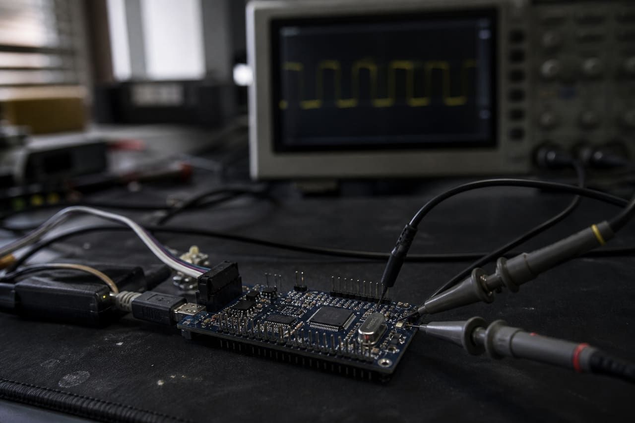
Embedded Firmware Development
Firmware that holds up in the field, not just on the bench
Layouts that pass signal integrity and manufacture cleanly
PCB layout is where a good schematic succeeds or fails. We route for signal integrity, thermal behaviour and EMI performance from the first placement decision rather than fixing it after a failed compliance test.
We work in industry-standard tools including Altium Designer, Cadence OrCAD and Mentor Graphics, and deliver fabrication and assembly packages that manufacturers can build without a query loop.
Discuss your project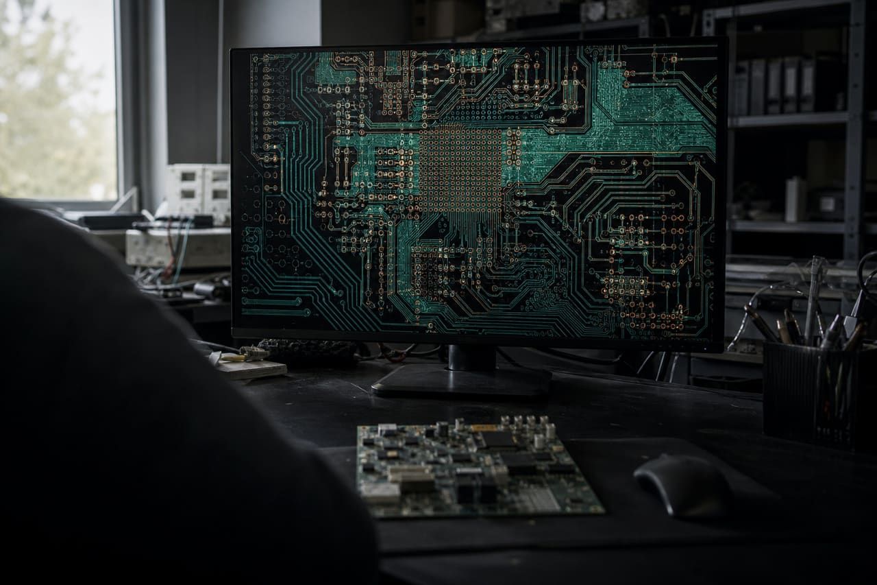
Translating circuit designs into placement and routing that respects the electrical intent.
Complex stack-ups with controlled impedance and disciplined power distribution.
DDR, PCIe, Ethernet and other high-speed routing with length matching and impedance control.
Placement and routing decisions that manage heat dissipation and reduce emissions.
Fabrication and assembly rules applied early so the board is production-ready on the first spin.
Support through fabrication, bring-up and test as the design moves to volume.
Layer stack-up, impedance targets and routing rules are agreed before placement. On high-speed designs this determines whether the board works, and it cannot be retrofitted.
Components placed for signal flow, thermal behaviour, manufacturability and test access — in that order of difficulty to change later.
Controlled-impedance routing with length matching where required, plus power distribution and return-path analysis rather than routing by rule-checker alone.
Design-rule and manufacturability checks, then a complete fabrication and assembly pack your manufacturer can build without a query loop.
We work across the major professional packages, including Altium Designer, Cadence OrCAD and Allegro, Mentor and KiCad. We will work in whichever tool your team already uses so the design stays maintainable in-house, and deliver source files in that format.
From two-layer boards through to dense multi-layer stack-ups with controlled impedance and blind or buried vias. The stack-up is chosen to meet the electrical requirement at the lowest sensible manufacturing cost, not to be impressive.
Yes, that is a common engagement. We will review the schematic first and raise anything that will cause layout or manufacturing problems, then take the design through placement, routing and manufacturing release.
The schematic, mechanical constraints such as board outline and connector positions, any impedance or high-speed requirements, and your manufacturer's capability file. If you do not have the last one, we will work to conservative rules that most fabricators can meet.
No account managers in the middle. Share your requirement and you will get a technical response, with an honest view of scope and timeline.
Start the conversationFirmware that holds up in the field, not just on the bench
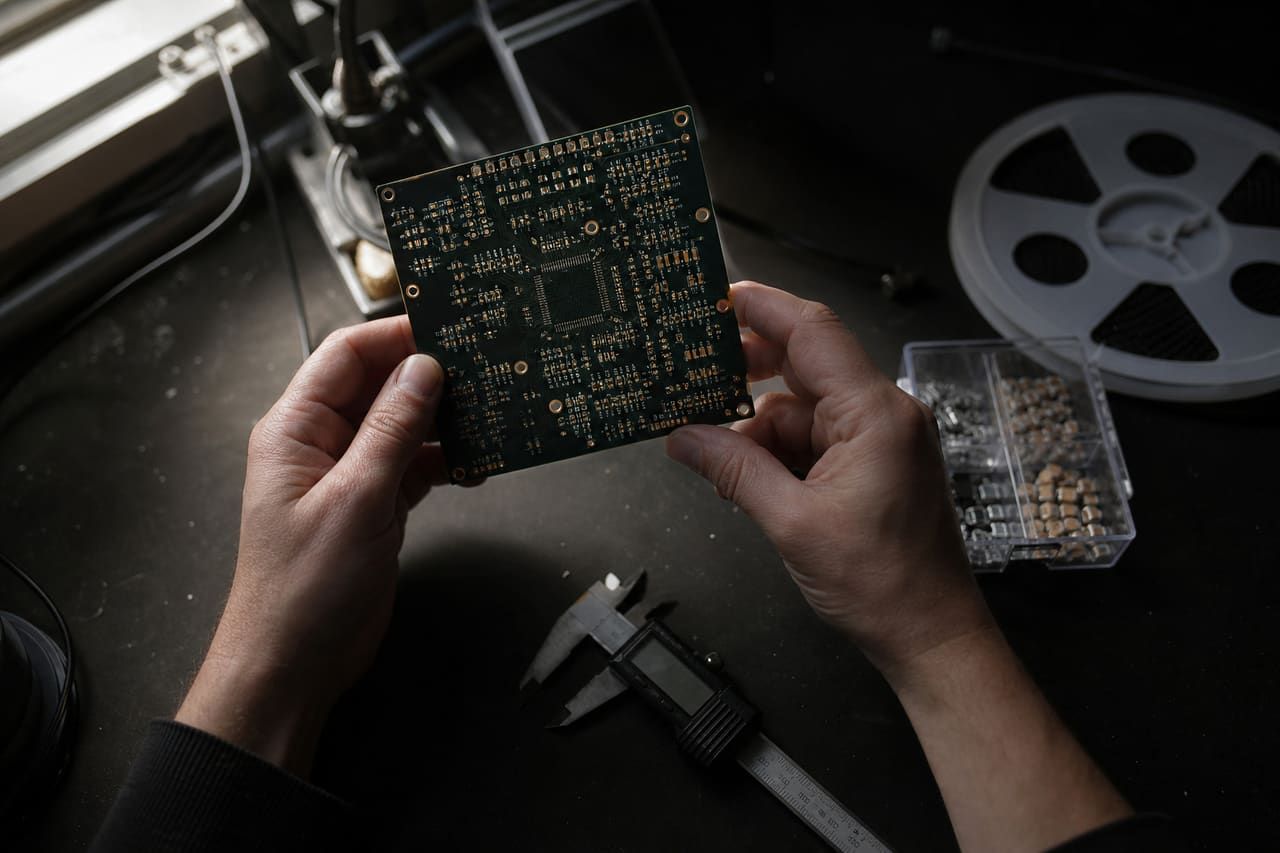
From schematic to a board that is ready to manufacture
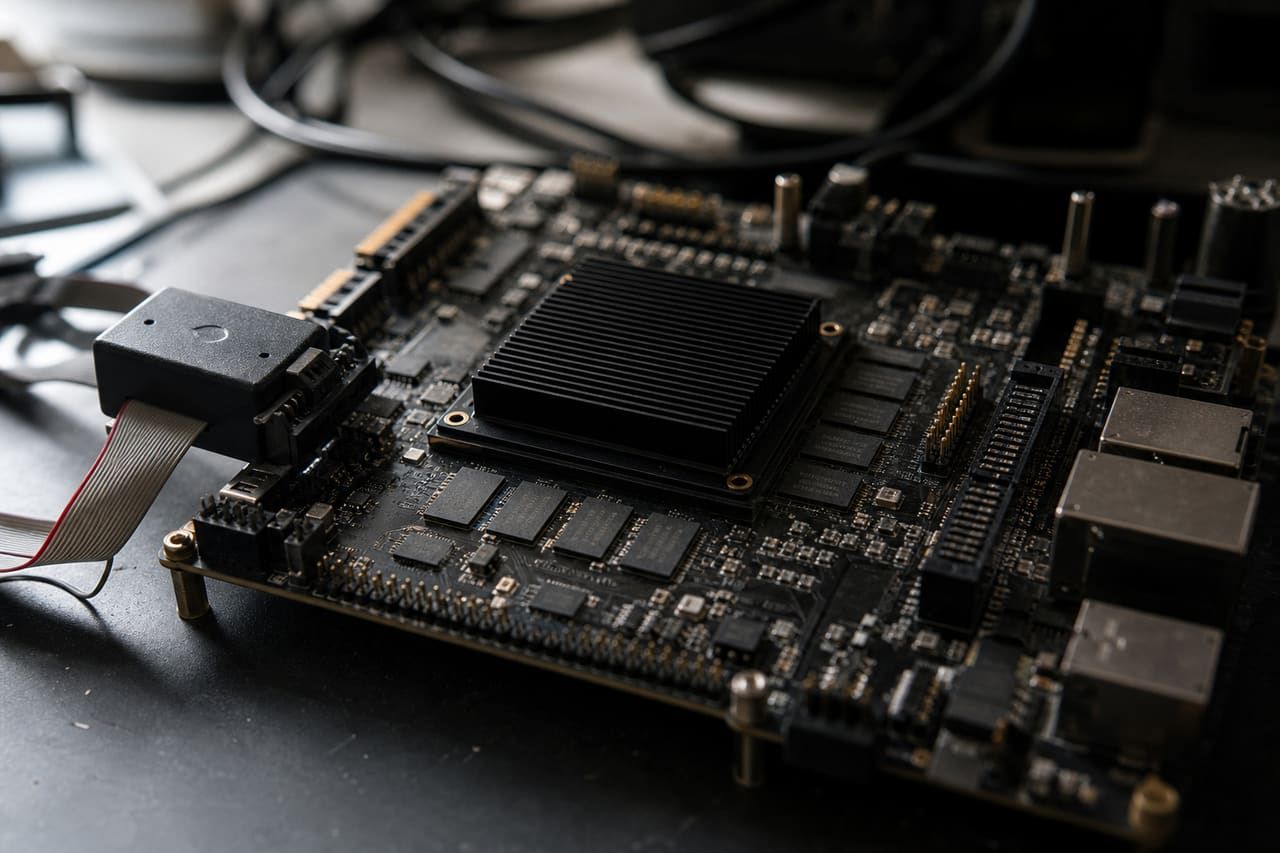
Custom digital logic, verified before it reaches silicon