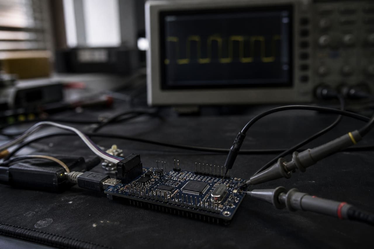
Embedded Firmware Development
Firmware that holds up in the field, not just on the bench
Custom digital logic, verified before it reaches silicon
When a workload will not meet its timing or throughput budget in software, we move it into logic. We design, verify and implement RTL for FPGA targets where determinism and parallelism matter more than raw clock speed.
Verification is treated as part of the design, not a phase bolted on at the end — functional simulation and timing analysis run alongside implementation so timing closure is not a late-stage scramble.
Discuss your project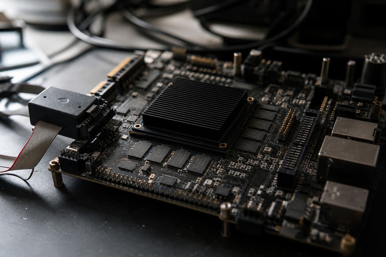
Logic designed from specification to implementation, optimised for area, power and timing.
Rapid hardware prototypes for validating architecture and de-risking downstream decisions.
Reusable, documented cores tailored to the application and its interfaces.
Functional simulation, timing analysis and directed testing to catch defects before hardware.
PCIe, DDR, Ethernet and comparable interface implementation and bring-up.
Power, timing and resource optimisation to fit the target device with margin to spare.
We establish what belongs in logic and what is better left in software, then set the throughput, latency and resource targets the design must meet.
Synthesisable RTL written for clarity and timing closure, with clock domain crossings identified and handled explicitly rather than discovered during integration.
Testbenches and directed tests developed alongside the RTL, so defects surface in simulation where they are cheap rather than on hardware where they are not.
Synthesis, place and route, and timing closure with margin, followed by hardware validation on the target board.
We work across AMD Xilinx, Intel Altera, Lattice and Microchip devices. Vendor choice is usually driven by the interfaces, resource requirements and long-term availability your product needs, and we are happy to advise on that selection.
That is the default assumption. The RTL is written for readability, documented at the interface and register level, and delivered with its testbenches so your team can extend it. We will run a handover session to walk your engineers through the architecture.
Yes. Where the same function is needed across products we develop it as a parameterised, documented and independently verified core, so it can be reused without being re-verified each time.
Verification is developed alongside the design rather than bolted on afterwards. That means directed and randomised testbenches, coverage tracking, and timing analysis across process corners before the design goes near hardware.
No account managers in the middle. Share your requirement and you will get a technical response, with an honest view of scope and timeline.
Start the conversationFirmware that holds up in the field, not just on the bench
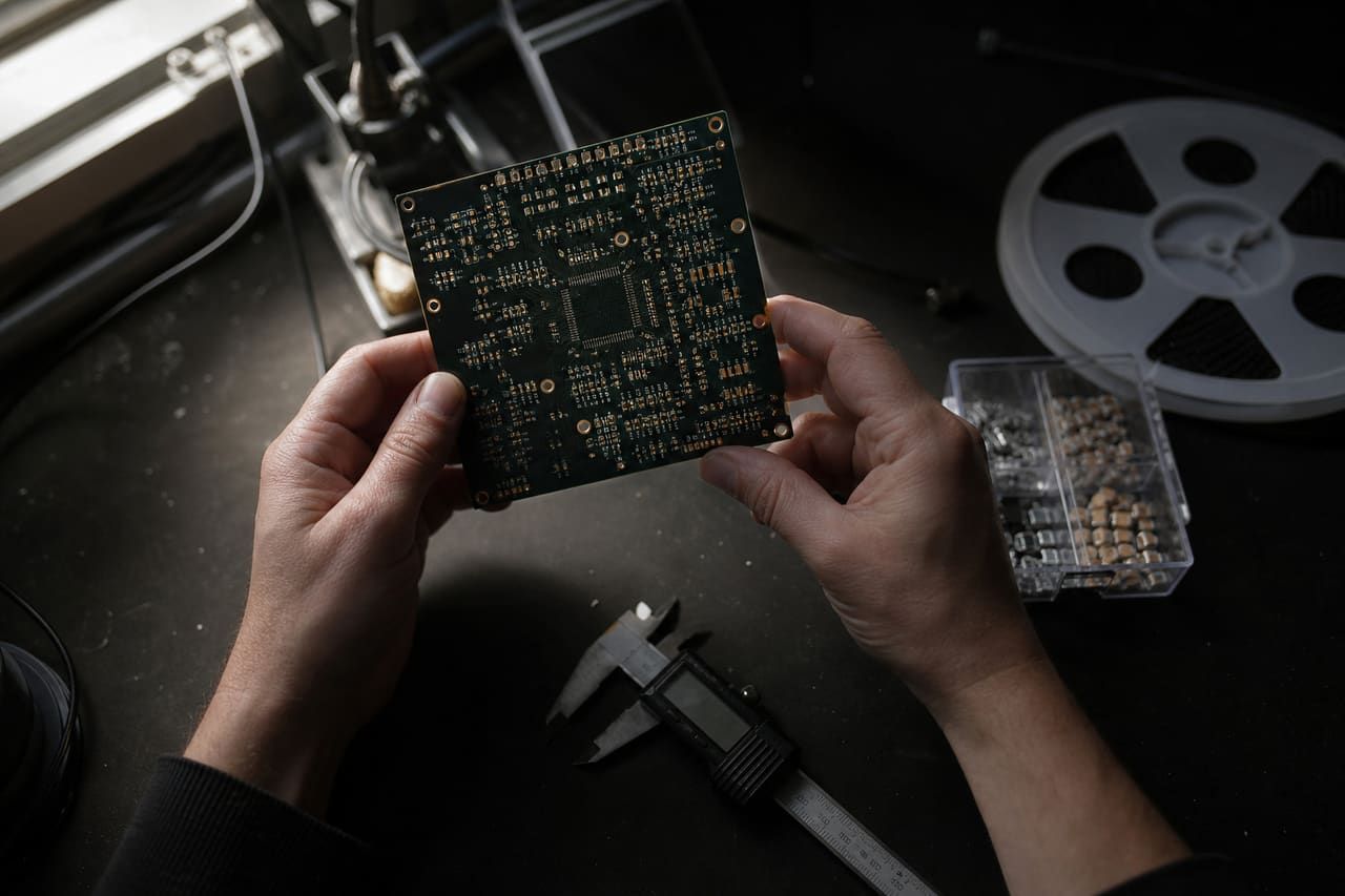
From schematic to a board that is ready to manufacture
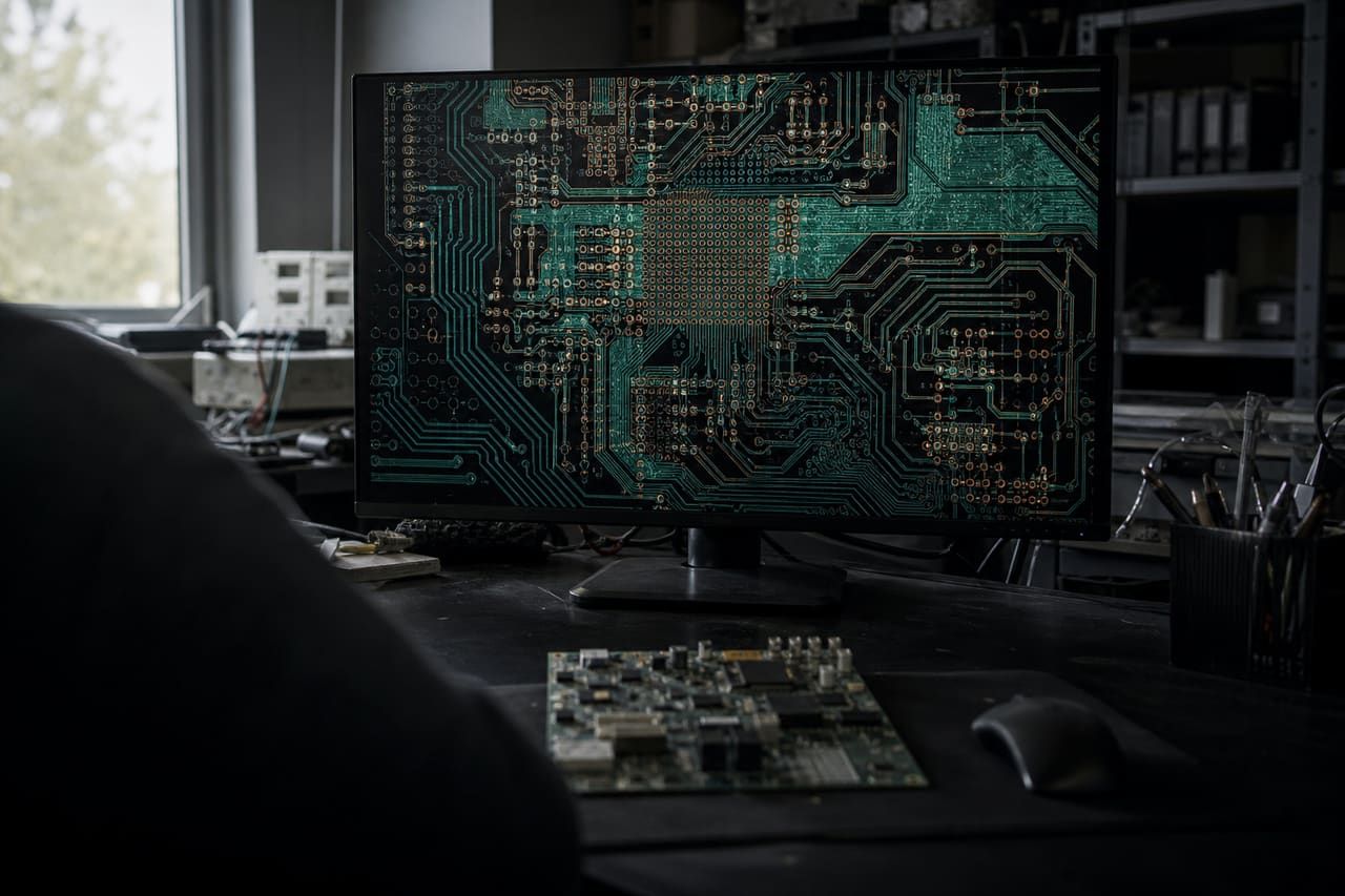
Layouts that pass signal integrity and manufacture cleanly